- 您现在的位置:买卖IC网 > Sheet目录3833 > AT80C51RA2-3CSUM (Atmel)IC 8051 MCU ROMLESS 40DIP
dsPIC33FJ32GP302/304,
dsPIC33F
J64GPX02/
X04,
AND
dsPIC
33FJ128GPX02/X04
DS70292G-p
age
56
2007-
2012
Microchip
T
echnolo
gy
Inc.
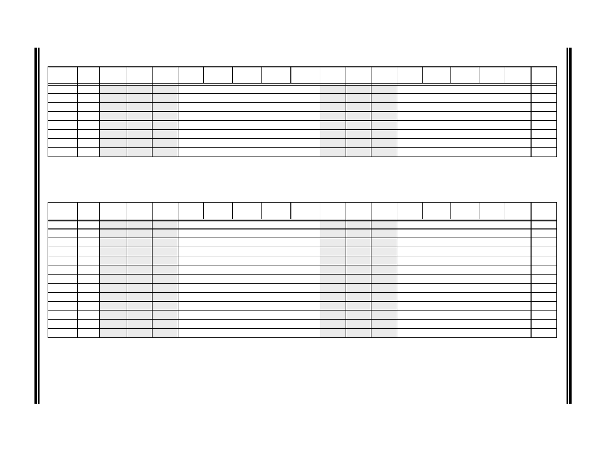
TABLE 4-22:
PERIPHERAL PIN SELECT OUTPUT REGISTER MAP FOR dsPIC33FJ128GP202/802, dsPIC33FJ64GP202/802 AND
dsPIC33FJ32GP302
File Name
Addr
Bit 15
Bit 14
Bit 13
Bit 12
Bit 11
Bit 10
Bit 9
Bit 8
Bit 7
Bit 6
Bit 5
Bit 4
Bit 3
Bit 2
Bit 1
Bit 0
All
Resets
RPOR0
06C0
—
RP1R<4:0>
—
RP0R<4:0>
0000
RPOR1
06C2
—
RP3R<4:0>
—
RP2R<4:0>
0000
RPOR2
06C4
—
RP5R<4:0>
—
RP4R<4:0>
0000
RPOR3
06C6
—
RP7R<4:0>
—
RP6R<4:0>
0000
RPOR4
06C8
—
RP9R<4:0>
—
RP8R<4:0>
0000
RPOR5
06CA
—
—RP11R<4:0>
—
RP10R<4:0>
0000
RPOR6
06CC
—
—RP13R<4:0>
—
RP12R<4:0>
0000
RPOR7
06CE
—
—RP15R<4:0>
—
RP14R<4:0>
0000
Legend:
x = unknown value on Reset, — = unimplemented, read as ‘0’. Reset values are shown in hexadecimal.
TABLE 4-23:
PERIPHERAL PIN SELECT OUTPUT REGISTER MAP FOR dsPIC33FJ128GP204/804, dsPIC33FJ64GP204/804 AND
dsPIC33FJ32GP304
File Name
Addr
Bit 15
Bit 14
Bit 13
Bit 12
Bit 11
Bit 10
Bit 9
Bit 8
Bit 7
Bit 6
Bit 5
Bit 4
Bit 3
Bit 2
Bit 1
Bit 0
All
Resets
RPOR0
06C0
—
RP1R<4:0>
—
RP0R<4:0>
0000
RPOR1
06C2
—
RP3R<4:0>
—
RP2R<4:0>
0000
RPOR2
06C4
—
RP5R<4:0>
—
RP4R<4:0>
0000
RPOR3
06C6
—
RP7R<4:0>
—
RP6R<4:0>
0000
RPOR4
06C8
—
RP9R<4:0>
—
RP8R<4:0>
0000
RPOR5
06CA
—
—RP11R<4:0>
—
RP10R<4:0>
0000
RPOR6
06CC
—
—RP13R<4:0>
—
RP12R<4:0>
0000
RPOR7
06CE
—
—RP15R<4:0>
—
RP14R<4:0>
0000
RPOR8
06D0
—
—RP17R<4:0>
—
RP16R<4:0>
0000
RPOR9
06D2
—
—RP19R<4:0>
—
RP18R<4:0>
0000
RPOR10
06D4
—
—RP21R<4:0>
—
RP20R<4:0>
0000
RPOR11
06D6
—
—RP23R<4:0>
—
RP22R<4:0>
0000
RPOR12
06D8
—
—RP25R<4:0>
—
RP24R<4:0>
0000
Legend:
x = unknown value on Reset, — = unimplemented, read as ‘0’. Reset values are shown in hexadecimal.
发布紧急采购,3分钟左右您将得到回复。
相关PDF资料
AT80C51RA2-3CSUL
IC 8051 MCU ROMLESS 40DIP
AT80C31X2-SLSUM
IC 8031 MCU ROMLESS 44PLCC
AT80C31X2-SLSUL
IC 8031 MCU ROMLESS 44PLCC
213300-2
CONN JACKSCREW PLUG 34 POS
AT80C31X2-RLTUM
IC 8031 MCU ROMLESS 44VQFP
AT80C31X2-RLTUL
IC 8031 MCU ROMLESS 44VQFP
AT80C31X2-3CSUM
IC 8031 MCU ROMLESS 40DIP
AT80251G2D-SLSUM
IC 8051 MCU ROMLESS 44PLCC
相关代理商/技术参数
AT80C51RA2-RLRUL
功能描述:8位微控制器 -MCU RLESS RA 40MHZ 3V COM TEMP RoHS:否 制造商:Silicon Labs 核心:8051 处理器系列:C8051F39x 数据总线宽度:8 bit 最大时钟频率:50 MHz 程序存储器大小:16 KB 数据 RAM 大小:1 KB 片上 ADC:Yes 工作电源电压:1.8 V to 3.6 V 工作温度范围:- 40 C to + 105 C 封装 / 箱体:QFN-20 安装风格:SMD/SMT
AT80C51RA2-RLSIV
制造商:ATMEL 制造商全称:ATMEL Corporation 功能描述:High Performance 8-bit Microcontroller
AT80C51RA2-RLTCL
制造商:IRF 制造商全称:International Rectifier 功能描述:High Performance 8-bit Microcontroller
AT80C51RA2-RLTCV
制造商:IRF 制造商全称:International Rectifier 功能描述:High Performance 8-bit Microcontroller
AT80C51RA2-RLTIM
制造商:IRF 制造商全称:International Rectifier 功能描述:High Performance 8-bit Microcontroller
AT80C51RA2-RLTUL
功能描述:8位微控制器 -MCU RLESS RA 40MHZ 3V COM TEMP RoHS:否 制造商:Silicon Labs 核心:8051 处理器系列:C8051F39x 数据总线宽度:8 bit 最大时钟频率:50 MHz 程序存储器大小:16 KB 数据 RAM 大小:1 KB 片上 ADC:Yes 工作电源电压:1.8 V to 3.6 V 工作温度范围:- 40 C to + 105 C 封装 / 箱体:QFN-20 安装风格:SMD/SMT
AT80C51RA2-RLTUM
功能描述:8位微控制器 -MCU RLESS RA 40MHZ 5V COM TEMP RoHS:否 制造商:Silicon Labs 核心:8051 处理器系列:C8051F39x 数据总线宽度:8 bit 最大时钟频率:50 MHz 程序存储器大小:16 KB 数据 RAM 大小:1 KB 片上 ADC:Yes 工作电源电压:1.8 V to 3.6 V 工作温度范围:- 40 C to + 105 C 封装 / 箱体:QFN-20 安装风格:SMD/SMT
AT80C51RA2-SLRUL
功能描述:8位微控制器 -MCU MICRO RLESS RA 40MHZ 3V COM TEMP RoHS:否 制造商:Silicon Labs 核心:8051 处理器系列:C8051F39x 数据总线宽度:8 bit 最大时钟频率:50 MHz 程序存储器大小:16 KB 数据 RAM 大小:1 KB 片上 ADC:Yes 工作电源电压:1.8 V to 3.6 V 工作温度范围:- 40 C to + 105 C 封装 / 箱体:QFN-20 安装风格:SMD/SMT